EECS151 Course Notes: Digital Design and a Three-Stage RISC-V Pipeline
In spring 2024 I took EECS151 (Introduction to Digital Design and Integrated Circuits, taught by Prof. J. Wawrzynek) together with its ASIC Lab as a visiting student at Berkeley. The lectures run from Verilog and FPGAs through the RISC-V ISA, memories, adders, and multipliers to place and route. The labs walk through a complete ASIC flow that covers RTL simulation, logic synthesis, place and route, and gate-level simulation after synthesis and after routing. Course materials and lab code live in 2024_spring_eecs151, and the final project lives in EECS151-Project.
Labs
The labs ran on the instructional servers, where Hammer drives Synopsys VCS and Cadence Innovus on the open SkyWater 130nm (sky130) process.
| Lab | Topic | My implementation |
|---|---|---|
| Lab 1 | Server environment and the Hammer tool flow | Setup screenshots |
| Lab 2 | RTL and gate-level simulation of an FIR filter, with waveforms read in DVE | Timing diagram and schematic analysis |
| Lab 3 | Splitting a GCD circuit into datapath and control, and building a divider | gcd_datapath.v, gcd_control.v, divider.v, and testbenches |
| Lab 4 | Wrapping the GCD unit as a coprocessor with FIFOs and ready/valid handshakes, plus an ALU | gcd_coprocessor.v, fifo.v, alu.v |
| Lab 5 | Dispatching requests to two GCD units through an arbiter, then place and route in Innovus | gcd_arbiter.v; after routing, all 64 timing paths meet their constraints with a WNS of 0 |
| Lab 6 | A vector dot product built on a single-port SRAM | dot_product.v and its testbench |
These labs drill one design habit: separate the datapath from the control first, then connect modules through ready/valid handshakes. Lab 3 asks for the values of A_reg and B_reg and their next-cycle values at every cycle of the GCD computation, and that exercise taught me to trace register transfers on paper before writing Verilog. In the post-route timing report of Lab 5, the paths with the smallest slack all start at the registers of the result FIFO and end at the A and B registers of the GCD datapath.
Final project: a three-stage RISC-V pipeline
For the final project, Timonty Chu and I designed a three-stage pipelined RISC-V processor and took it through synthesis and place and route on sky130 with Hammer. The project had four checkpoints and a final checkoff, the Verilog comes to about 2,300 lines, and synthesis targeted a 20 ns clock period.
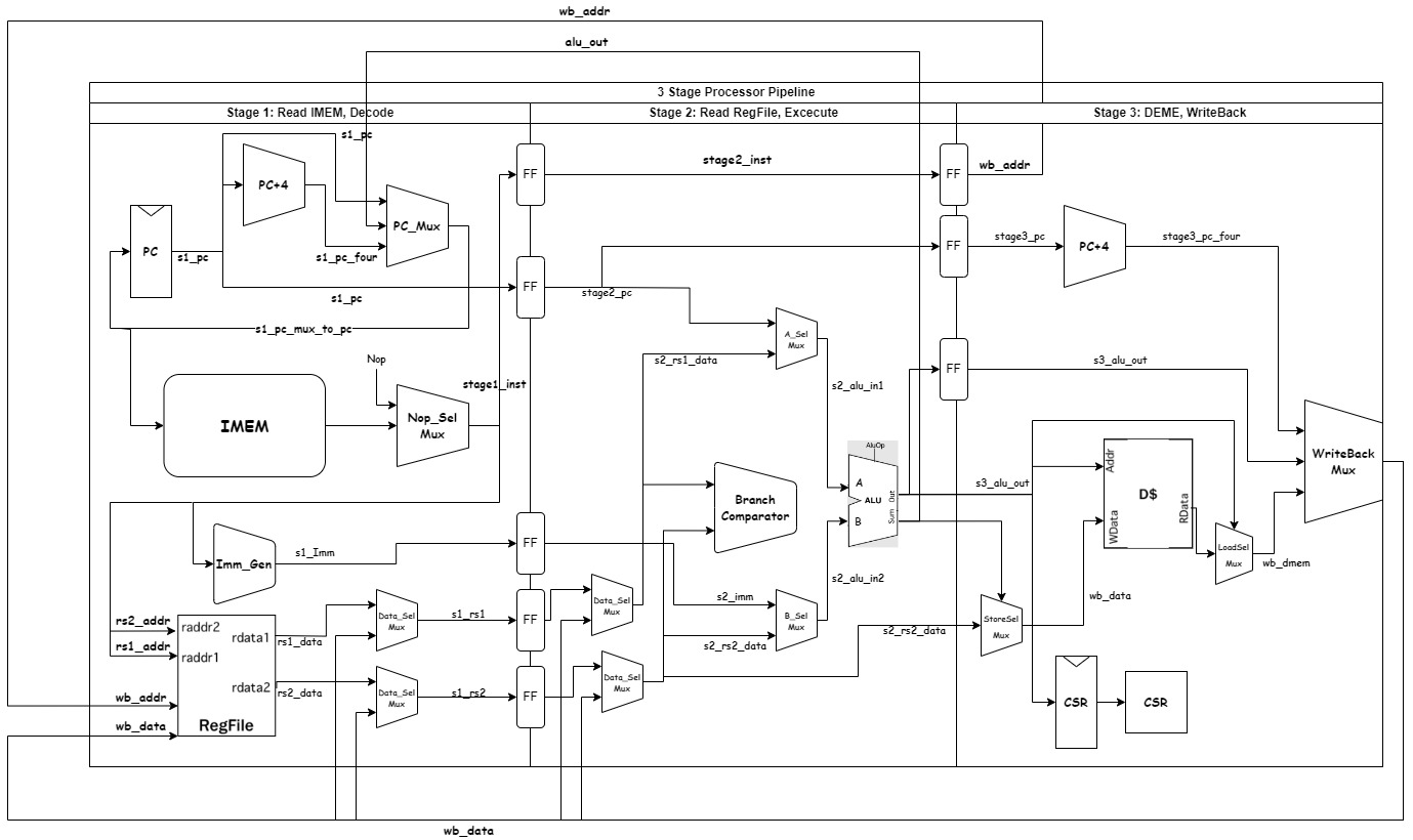
The pipeline splits the work into three stages:
- Stage 1: reads IMEM, decodes the instruction, generates the immediate, and reads the register file.
- Stage 2: selects the ALU operands and executes, while the branch comparator resolves the branch in the same stage.
- Stage 3: accesses the data cache, selects the load result by access type, writes back to the register file, and writes the CSR.
Three parts of the implementation needed particular care:
- Data hazards: a set of
Data_Selmultiplexers at the operand inputs of stages 1 and 2 forwards the writeback data to later instructions. - Control hazards: jumps resolve in stage 2, and the instruction already fetched into stage 1 is replaced with a nop through
Nop_Sel. - Memory stalls: cache reads return one cycle late, so after loads and on icache or dcache misses the
StallHandlerstalls the PC and the pipeline together.
The data cache is direct-mapped and write-back, with 64 lines of 512 bits each and a dirty bit per block.
For testing, we started with randomized stimulus in Verilog testbenches, then extended the Python script ALUTestGen.py to generate test vectors for R-type and I-type instructions and checked them one by one through $readmemb. After RTL verification, the design still had to pass gate-level simulation after synthesis and again after routing.
2026.09.28